
Overview of research topic
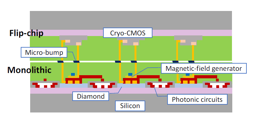
3D Integration of diamond quantum systems
The 3D integration employs multiple vertically stacked active layers for higher integration density and functionalities. Compared to conventional electronic chips, quantum computer (QC) chips are versatile, but more demanding and challenging in many ways; new materials, cryogenic operation temperature and unconventional circuit operation.
In this work, we propose a 3D integration process for implementing a modular QC chip with diamond spin qubits in a combination of monolithic and flip-chip integration techniques. This integration scheme is based on using directly bonded diamond chips, which provides a diamond-on-silicon (DOS) platform. A monolithic integration of photonic circuits, waveguide coupled single-photon detectors, local magnetic field generators is carried out on this DOS substrate. The cryo-CMOS control chip is separately manufactured and then bonded with the monolithic integrated chip with a flip-chip technique. The bonding is achieved using superconducting micro-bumps with niobium nitride (NbN).
Check our latest publication: doi.org/10.1109/IEDM19574.2021.9720552
3D integration of modular quantum computer chip with spins in diamond.
Diamond-on-silicon direct bonding
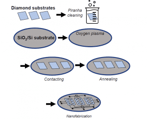
Direct bonding process flow of diamond-on-silicon (DOS)
Most diamond substrates are made by high-pressure, high-temperature (HPHT) methods, where the maximum size of readily available single crystalline diamond substrate with a low impurity level is very small. This limitation prevents the use of an advanced semiconductor manufacturing line which accepts a wafer size of at least 2 inches. Another challenge is the removal of dislocation defects in a reasonable thickness and growth time.
As an alternative, direct bonding of single crystalline diamond substrate on silicon (DOS) is a promising approach. Here, the diamond substrate is treated with Piranha solution and the surface is hydroxylated and then bonded with oxygen-plasma-activated silicon wafer, without pressure, under atmospheric conditions. The bonded samples are annealed at 200 °C to strengthen the bonding. This method is encouraging for the preparation of a DOS wafer, which enables large-scale nanostructures in diamond. The rest of the active layers can be fabricated monolithically or vertically stacked in a chip level.
Pick-and-place integration of vacancy centers in diamond
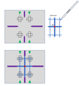
Steps for pick-and-place of diamond photonic structures.
An alternative approach to wafer bonding is hybrid integration, where different materials can be connected together without chemically bonding them. The hybrid integration process that offers the highest yield is pick-and-place.
The focus of this research is to integrate the diamond chip containing the vacancy center onto a photonic chip using the pick and place process. This requires the design of a diamond cross waveguide structure, the taper at the edges of both the diamond and the silicon nitride waveguides and the support structure of the diamond chip.
Photonic structures
To mediate interactions between different qubits in diamonds, a promising approach is creating an on-chip quantum network in which color centers interact optically via nanophotonic interconnects. The use of photonic structures plays a crucial role in this implementation, by enhancing the photon emission into the zero-phonon line (ZPL).
In this research, we design suitable photonic structures and simulate their performance. These devices will later be fabricated in the cleanroom and, subsequently, characterized.
Superconducting nanowire single-photon detectors (SNSPD’s)
SNSPD characterization setup.
Efficient detection of single-photon emission is a vital aspect in the design of quantum computers based on color centers in diamond. SNSPD’s are the best candidate for this purpose, showing high detection efficiencies in combination with a low dark-count rate.
Typically, SNSPD’s and qubits are separated from each other, connected by optical fibers. The goal, however, is to integrate all subsystems of the quantum computer on a single chip, which includes the SNSPD’s. On-chip fiber connections are, of course, not practical, so waveguide structures are used instead. SNSPD’s are placed on top of these structures. As the light travels through the waveguides, the photons are absorbed by the nanowire, resulting in a detection event.
A challenge that arises with integration is the change in operation environment. Color center qubits require biasing with a high static magnetic field. On-chip integration of both qubit and detector requires the SNSPD’s to operate in this magnetic field as well. This requires optimization, since magnetic fields alter the properties of superconducting nanowires.
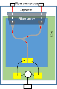
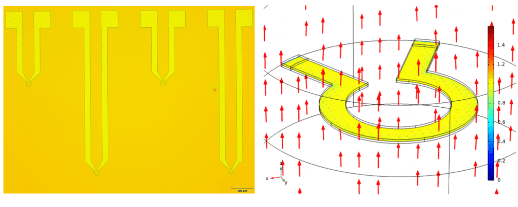
Magnetic-field generator
The nitrogen-vacancy (NV) center has a total spin of S=1 in its negatively charge state. This allows us to modify its energy levels by applying a magnetic field B, by means of the Zeeman splitting, making them the basis for a quantum bit.
A local magnetic field with a good control can address the qubits separately by tuning the splitting. On-chip inductors can be used to locally generate static magnetic fields in an integrated circuit platform.
In this work, we explore and propose the design of effective on-chip coils for generating local and uniform static magnetic fields. The figure of merits of the on-chip coils is determined by their material properties, geometries or layout and the technological parameters. Here, we propose the implementation of on-chip coils using superconducting materials (NbN or NbTiN). The MFGs with a combination of cryo-CMOS electronics will allow manipulation of defect spin qubits in diamond efficiently, in a scalable architecture.
Measuring cancerous cells with NV centers
Laser irradiation on an NV layer in diamond, with a bio-sample placed on top. Fluorescence collection using the objective lens of an ODMR setup.
Nitrogen-vacancy (NV) centers are popular tools for measuring magnetic fields at room temperature. These carbon point defects correlate magnetic field strength with photoluminescence. NV centers can be used to define the weak magnetic fields of biomaterials, like cancer cells.
In this project, we investigate the creation of an enhanced setup able to measure such cells labelled with magnetic nanoparticles. The final goal is to be able to accurately distinguish between cancerous and healthy cells.
On-chip quantum sensing
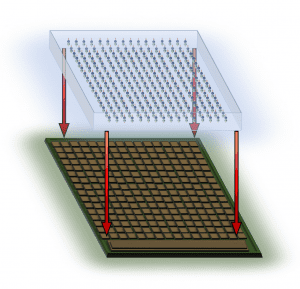
Diamond substrate containing array of single NV-centers integrated in SPAD array chip.
This project focuses on the CMOS integration of Nitrogen-Vacancy (NV) centers in diamond, into an on-chip platform. The goal is to create a compact, high-sensitivity quantum sensor.
First, the diamond substrate goes through various cleanroom processes. After the exposure and development of sufficiently small (nm-sized) holes, the substrate undergoes nitrogen implantation and annealing. This way, an array of single NV centers is fabricated. Meanwhile, we design an array of single-photon avalanche diodes (SPAD) in 40 nm CMOS technology (TSMC). These photon detectors can operate at room temperature; a great benefit when aiming for biological applications.
Finally, by making use of ODMR measurement techniques, we will be able to perform magnetic field sensing for bio-imaging applications. Thus, the integration of these SPADs on our diamond will provide even more accurate measurements, further increasing the platform’s detection efficiency and sensitivity.
Machine learning for quantum control and data processing
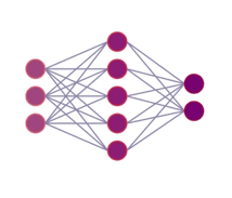
Fully connected network with one input, one hidden and one output layer.
Recently, deep learning has slowly been applied to the field of quantum control and data processing, owing to numerous successes in industry so far.
Quantum optimal control, like state steering and gate design, can benefit from utilizing deep reinforcement learning. More specifically, it is now possible to perform optimization directly on an experimental platform, rather than pure numerical optimization on a computer, in which real world environmental noises are directly incorporated during the optimization.
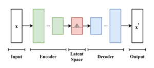
The architecture of a simple autoencoder.
On the other hand, neural network models like autoencoder can help with denoising experimental data and, subsequently, make it a lot easier to perform data processing or extract hidden information that was extremely difficult to find in the past. When combined with generative models or simple classification models, it is possible to make an end-to-end deep learning pipeline for both pre and post processing data analysis.
Levitated micromagnets for quantum sensing
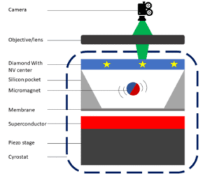
Levitated micromagnet setup for quantum sensing.
Mechanical oscillators are used in a wide range of applications as force and inertial sensors. The use of a levitated mechanical oscillator based on magnetostatic fields avoids multiple losses and problems others have. Combining this with an NV center to create strong spin-mechanical coupling is a promising candidate for quantum sensing, quantum communication and ultra-sensitive magnetometry.
The oscillator consists of a micromagnet contained in a silicon pocket that is levitated with a type II superconductor. The lid of this pocket is a diamond containing NV centers for spin-mechanical coupling. NV centers are fluorescent and when coupled to the magnet the intensity depends on the magnets position. Displacements can thus be precisely determined by measuring the fluorescence of the NV center.
In this research, micromagnets that range from 1 to 100 μm are levitated with the use of a type II superconductor. The Q-factor, trapping frequencies and coupling strength will be measured for the different sizes of micromagnets.