
Our Device Engineers strive to deliver devices with ever improved reliability and yield for our projects. We have found that success requires multiple activities. The first is to translate device requirements from System Engineers into circuit designs fabricated with suitable materials. The second is to closely monitor fabrication runs for process control, and to systematically record data from individual process steps into a database. Because new materials and new circuit designs can often come with surprises, a methodology for quick measurement on relevant test-devices is critical. Our team of experts in measurement and fabrication therefore work closely with other scientists and engineers with the System, Software, Cryogenic, and Optical groups. There are Quantum Device Engineers active in all divisions of QuTech, and the devices we deliver represent the heart of the experimental quantum research program.
Projects we contribute to
Growth
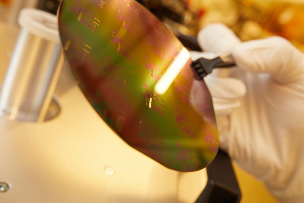
Spin qubits require the localization of single electrons (or single holes) within electrostatically defined regions of semiconductors. This charge carrier confinement is achieved in two dimensions by metallic gates, deposited on the surface, that can tune the electrochemical potential of the semiconductor below it. Confinement of the electron (or hole) in the vertical dimension is achieved by growing very thin layers or Si (or Ge) several tens of nanometers below the surface of a SiGe matrix. These layers must be grown with incredibly high purity because crystalline defects and/or interfacial roughness can cause the electrons or holes to lose coherence. Our engineers and researchers collaborate in growing some of the best quality material stacks in the industry, and this is a key enabler for high quality spin qubit devices.

Ge/Si based devices
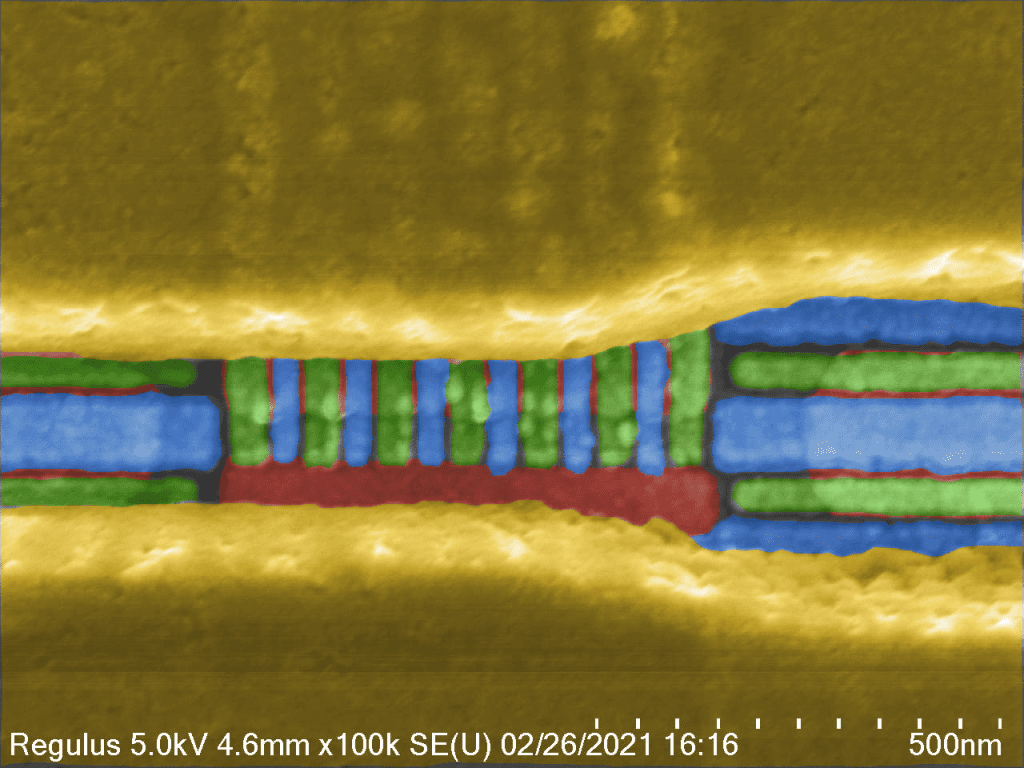
In order to run a quantum computing algorithm with electrons (or holes) isolated within semiconductor devices, the spin of these charge carriers needs to be manipulated and neighboring charge carriers must undergo controlled interactions. This is achieved by tuning the electrochemical potential of the carriers using ultra small metal gates on the surface of the device. The fabrication of these metal lines, as well as the surrounding dielectric and magnetic materials, must therefore be highly controlled and reproducible. Our engineers have been working to standardize the fabrication processes using CMOS techniques and fast turnaround measurement protocols. An in-depth understanding of the fabrication processes, and how they affect material purity, is critical for achieving sufficient numbers of high-performance devices. The best of these devices are passed on to our researchers, or placed within QuTech’s Quantum Inspire quantum computing demonstrator system, for scientific experiments.
Diamond based devices
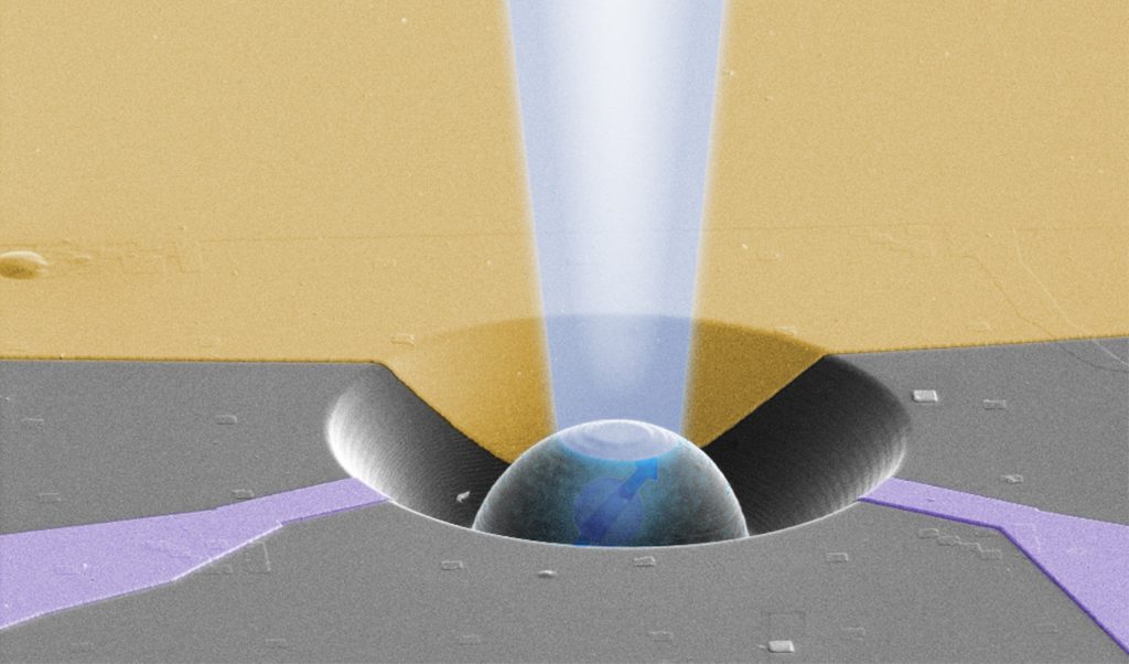
Achieving the goal of a quantum internet requires coherently transferring quantum information between two different, physically remote, locations. Each host location has a diamond qubit chip, and optical photons are used to connect them. Several microns below the surface of the diamond exists an optically active defect site comprised of a nitrogen atom positioned next to a carbon vacancy site. A critical aspect is therefore enhancing the coupling of photons from free space into this defect center below the diamond surface. Fabrication engineers, quantum optics physicists, and system engineers work together on optimizing diamond-based devices for these applications. First, a suitable nitrogen-vacancy defect site needs to be identified by optical inspection of the bulk diamond. Next, the bulk diamond material surrounding the defect is milled away into a micron-sized lens that enhances optical coupling to it. Finally, electrical lines must be fabricated in close proximity to the lens to allow for electrical control of the vacancy center. Millimeter-sized diamond pieces of sufficient quality are very rare, and fabrication on such substrates is not industry standard. Fabrication engineers are working hard to define robust processes that increase yield, reliability, and performance of these highly precious devices.
Join us in creating the quantum future
Work with us as an employee or partner
Learn more
Engineering expertises
Quantum technology is among the most far-reaching and challenging technologies of our time. To address this challenge, our researchers and engineers from different divisions work closely together to optimize our research projects. Interdisciplinary collaboration is crucial for making the next steps in developing scalable prototypes of a quantum computer and an inherently safe quantum internet.