

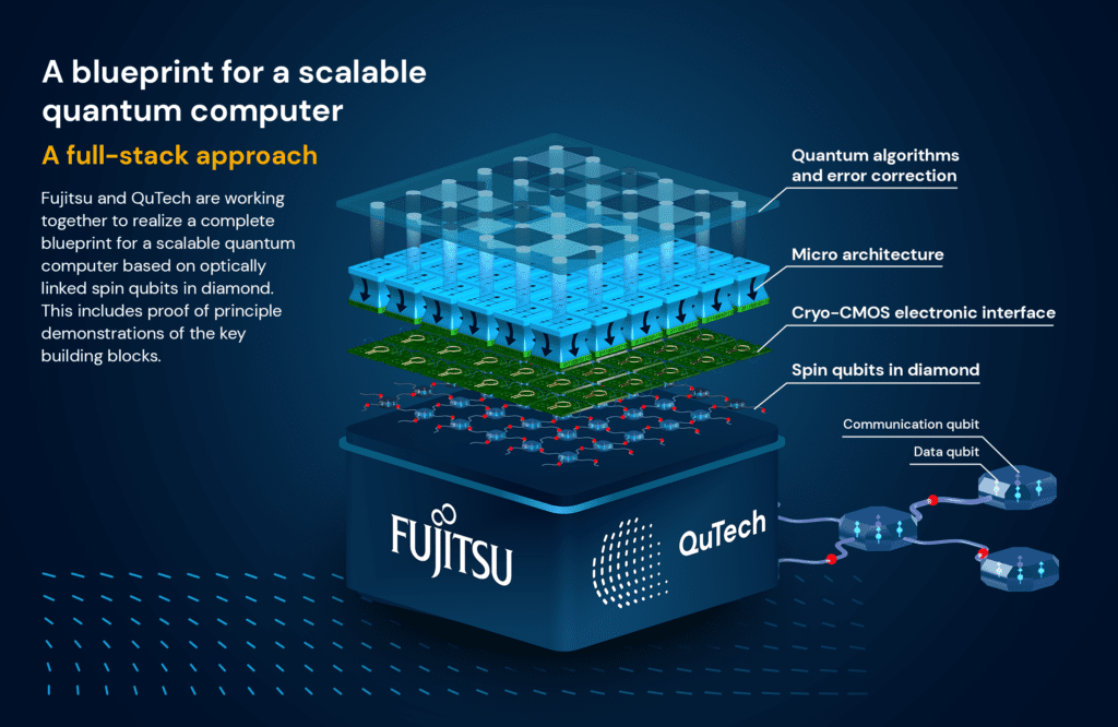
To develop this blueprint we will take a full-stack approach: we will realize the qubit modules, design the interface electronics and the micro architecture, develop wafer-scale 3D integration and integrated optics, perform benchmark proof-principle quantum algorithms and error correction codes, and perform a system engineering analysis to combine these components into a complete blueprint.
Quantum algorithms and error correction
The top layer consists of quantum error correction and algorithms implementing the quantum computational logic. It uses error-correction codes to counteract the inherent instability of quantum states, and designs algorithms that effectively leverage the qubits to solve in principle some complex problems significantly faster than classical computers.
Micro architecture
The micro architecture provides a functional abstraction of the underlying electronic interface. It allows for the translation of the quantum algorithms and error-correction to fine-grain digital control signals for the electronic interface.
Cryo-CMOS electronic interface
The cryo-CMOS electronics exploit commercial semiconductor technology to fabricate integrated circuit operating close to the qubits, hence at a similar cryogenic temperature. The cryo-CMOS interface comprises the generation of the magnetic fields to bias the qubits and operate on them, the readout of the photon detectors, and the controller of the photonic components.
Spin qubits in diamond
The qubit layer consists of modules containing robust electron and nuclear spin qubits hosted in diamond. These 5-10 qubit modules are coupled to each other and to optical control fields via on-chip photonic integrated circuits, enabling modular scaling of the quantum processor.
This project is a collaboration between QuTech and Fujitsu, co-financed by Holland High Tech with a PPP allowance for research and development in the top sector HTSM and a PPP allowance for research and innovation from the Ministry of Economic Affairs – project codes TKI HTSM 24.0102 and RVO PPS 23-2-03586828.
 QuTech / TU Delft, Fujitsu Project Team