19.05.2020Uncategorized
New setup for high-throughput electrical measurements of quantum materials and devices

Researcher

New setup for high-throughput electrical measurements of quantum materials and devices
QuTech, a collaboration between TU Delft and TNO, has demonstrated a novel setup for fast turnaround testing and validation of quantum materials and devices. The setup uses ordinary electronic chip components that can operate at extreme cryogenic temperatures, and can be readily integrated in any type of cryostat. The scientists have published the details of their setup in an open-access journal, allowing research groups worldwide to modify their cryostat and greatly enhance its throughput.
Principal investigator Giordano Scappucci, together with first authors Paquelet Wuetz and Bavdaz and the rest of his team, have built a new setup that drastically cuts the time needed to develop quantum materials and devices. The setup increases the number of wires that can operate at cryogenic temperatures in the cryostat by an order of magnitude, while keeping the same number of wires operating at room temperature. This is an important accomplishment for the electrical measurement of large quantum systems, where a limited number of wires operating at cryogenic temperatures can form an input/output bottleneck. The new cryogenic platform also holds promise for scaling-up quantum technology due to its capacity to test and validate multiple chips together.
To prove the value of the setup, the scientists, in collaboration with Intel, used the cryogenic platform to accelerate the industrial development of “strained-silicon quantum wells”: thin layers of semiconductor silicon stretched and sandwiched between layers of silicon-germanium. The scientists trapped electrons in these quantum wells and then measured the electrical transport properties of these electrons at extreme cryogenic temperatures. The investigated material platform showed remarkable properties for making high-quality spin qubits, which form the building blocks for a spin-based quantum computer.

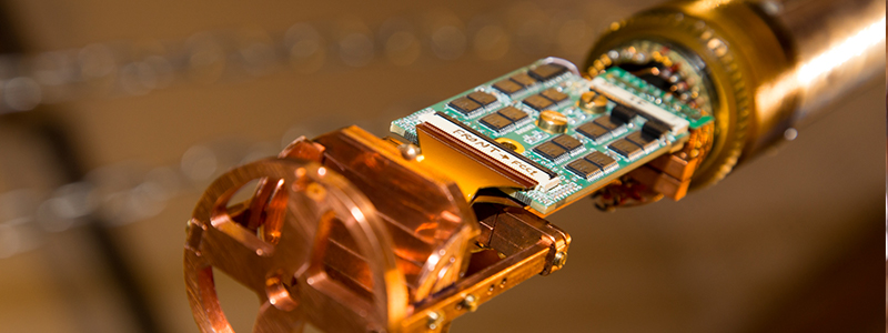
The setup, a cryogenic multiplexer platform, can test and validate multiple chips together in one cool-down at a temperature of 50 mK.
The cryogenic multiplexer platform is easy to integrate in any kind of cryostat and is based on a common off-the-shelf CMOS multiplexer (an ordinary chip component that controls its output signal based on the input signals that it receives). The details of the platform have been published in an open-access journal. By doing so, they want to empower research groups worldwide to dramatically augment the throughput of their cryostat at negligible cost.
Publication
Multiplexed quantum transport using commercial off-the-shelf CMOS at sub-kelvin temperatures
B. Paquelet Wuetz, P.L. Bavdaz, L.A. Yeoh, R. Schouten, H. van der Does, M. Tiggelman, D. Sabbagh, A. Sammak, C.G. Almudever, F. Sebastiano, J.S. Clarke, M. Veldhorst and G. Scappucci
npj Quantum Information, available online 19 May 2020
DOI: 10.1038/s41534-020-0274-4; https://www.nature.com/articles/s41534-020-0274-4
Image credits
Both photos of the setup are free to use, credit M. Lodari for QuTech